Lam Research Announces Plans to Invest More than $3B to Expand Global Lab Network, Increase Innovation Velocity in the AI Era
FREMONT, Calif., Aug. 13, 2026

Press Release Disclaimer: This is a press release distributed through the XPR Media network. It has not been independently verified by our newsroom.

Lam Research Announces Plans to Invest More than $3B to Expand Global Lab Network, Increase Innovation Velocity in the AI Era
PR Newswire
FREMONT, Calif., Aug. 13, 2026
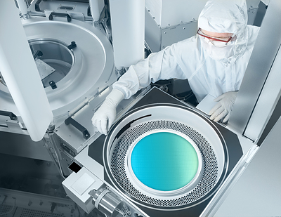
FREMONT, Calif., Aug. 13, 2026 /PRNewswire/ — Lam Research Corp. (NASDAQ: LRCX) today announced that it intends to invest more than $3 billion over the next five years to expand its global research and development (R&D) lab network. The planned multi-site expansion is expected to add infrastructure and capabilities to increase experiment capacity by more than 50%. Lam’s R&D approach combines specialized labs worldwide, each purpose-built to accelerate a distinct step of the innovation cycle, with deep customer collaboration that includes locations near customer facilities. Together, Lam’s labs operate as an integrated 24/7 network, enabling innovation in parallel and at scale. With this investment, Lam intends to further compress product development cycles for customers, from pathfinding to fab deployment.
“In the AI era, the pace of innovation is relentless, requiring chips with new architectures, different materials, and complex features engineered with nanoscale precision. Our ability to increase velocity throughout the R&D process has become a decisive advantage,” said Tim Archer, president and chief executive officer of Lam Research. “We are investing with the intention of staying ahead of what our customers need, further strengthening our global innovation engine to deliver the next generation of semiconductor breakthroughs.”
Lam’s global lab network spans the United States, Asia, and Europe. The combined R&D infrastructure supports more than one million experiments annually. Facilities specialized for foundational research in new chemistries, materials and mechatronics have the capability to compress weeks of experimental work into as little as a few days in many cases. Process development labs carry those advances toward production readiness, with engineering, product development and manufacturing teams working side by side on the same tools. Located in proximity to customers, Lam’s technology centers support rapid qualification and validation alongside customers’ engineering teams.
The integrated lab network enables tools, data and expertise to be shared across locations and time zones, so a discovery in one lab becomes knowledge every lab can use. In recent customer engagements, this approach has enabled Lam to shorten process development up to 2.5 times.
“Congratulations to Lam on this investment. Micron is proud to work with Lam as we advance memory and storage solutions that power the AI ecosystem,” said Scott DeBoer, executive vice president and chief technology and products officer at Micron Technology. “Our longstanding collaboration with Lam continues to drive innovation in leading-edge front-end and advanced packaging technologies, and we look forward to building on this momentum to scale AI across the semiconductor ecosystem.”
“Wafer-level semiconductor device processing is the backbone of all semiconductor ecosystems and the enabler of subsequent chip technology advancements,” said John West, chief analyst, Semiconductor Equipment at Yole Group. “AI-related investment is lifting demand for deposition and etch intensity. Lam Research’s etch, deposition, and advanced packaging wafer fabrication equipment innovations along with new EUV/DUV lithography technologies have helped to enable the production of semiconductor devices with the right combination of power consumption, performance, price, and form factor to unlock the AI revolution. Sustaining this momentum will require the semiconductor ecosystem to innovate faster, compress development cycles, and scale new technologies into manufacturing more quickly.”
Lam plans to begin expanding the global lab network this year with the goal of increasing innovation velocity.
Additional Media Resources
- Lam Blog, How Deposition and Etch Are Reshaping Chips for the AI Era
- Visit Lam’s Media Center for images and visual assets
About Lam Research
Lam Research Corporation (NASDAQ: LRCX) is a global supplier of innovative wafer fabrication equipment and services to the semiconductor industry. Lam’s equipment and services allow customers to build smaller and better performing devices. In fact, today, nearly every advanced chip is built with Lam technology. We combine superior systems engineering, technology leadership, and a strong values-based culture, with an unwavering commitment to our customers. Lam Research is a FORTUNE 500® company headquartered in Fremont, California, with operations around the globe. Learn more at www.lamresearch.com.
Caution Regarding Forward-Looking Statements
Statements made in this press release that are not of historical fact are forward-looking statements and are subject to the safe harbor provisions created by the Private Securities Litigation Reform Act of 1995. Such forward-looking statements relate to, but are not limited to: our intention to invest more than $3 billion in the next five years to expand our R&D lab network across multiple sites, compress product development cycles for customers, and stay ahead of customer needs and strengthen global innovation to deliver the next generation of semiconductor breakthroughs; our expectation to add infrastructure and capabilities to increase experiment capacity by more than 50%; our ability to accelerate the innovation cycle; the requirement in the AI era for chips with new architectures, different materials, and complex features; the advantages associated with our ability to increase velocity throughout the R&D process; the effects of Micron’s relationship with Lam; Yole Group’s views regarding AI-related investment lifting demand for deposition and etch intensity and that sustaining momentum will require faster innovation, development cycles, and new technology scaling; our plan to begin expanding our lab network with the goal of increasing innovation velocity; and our unwavering commitment to customers. These statements are not a guarantee of future performance and involve a number of risks, uncertainties, and other factors that could cause our actual results or outcomes, or the timing of our results or outcomes, to differ materially from those expressed or implied in this press release. Such risks, uncertainties, and other factors include: our ability to successfully execute the planned expansion of our global R&D lab network; our ability to achieve the anticipated benefits of our investments in R&D infrastructure; the timing, cost, scope, and anticipated benefits of planned R&D investments may differ from our expectations; business, economic, political and/or regulatory conditions in the consumer electronics industry, including wafer fabrication equipment spending, the semiconductor industry and the overall economy may deteriorate or change; the actions, performance, or investment levels of our customers and competitors may be inconsistent with our expectations; customer and product mix, including across market segments and geographical regions, may change; we may be unable to effectively manage and implement pricing actions, realize the value of our products and technology, successfully commercialize new products and technologies, or execute on perceived opportunities; we may be unable to achieve anticipated operational, manufacturing, supply chain, procurement, and scale efficiencies; customer technology transitions, capacity expansions, and fab construction projects may have different timing or be less successful than we expect; we may be unable to manage operating expenses effectively while continuing to invest in R&D, product innovation, customer support, and future growth opportunities; trade regulations, export controls, tariffs, trade disputes, and other geopolitical developments may inhibit our ability to sell our products; supply chain cost increases, tariffs, and other inflationary pressures have impacted and may continue to impact our profitability; supply chain disruptions or manufacturing capacity constraints may limit our ability to manufacture and sell our products; natural and human-caused disasters, disease outbreaks, war, terrorism, political or governmental unrest or instability, or other events beyond our control may impact our operations and revenue in affected areas; as well as the other risks and uncertainties that are described in the documents filed or furnished by us with the Securities and Exchange Commission, including specifically the Risk Factors described in our most recently filed periodic reports on Form 10-K and Form 10-Q and subsequent filings. You should evaluate all forward-looking statements made in this press release in the context of these risks, uncertainties, and other factors. Readers are cautioned not to place undue reliance on these forward-looking statements, which speak only as of the date hereof and are based on our, Micron, or Yole Group’s current beliefs, expectations, and assumptions about future events. Except as required by law, we undertake no obligation to update the information or statements made in this press release.
Company Contacts
Laura Bakken
Public Relations
(510) 572-9021
publicrelations@lamresearch.com
Ram Ganesh
Investor Relations
(510) 572-1615
investor.relations@lamresearch.com

 View original content to download multimedia:https://www.prnewswire.com/news-releases/lam-research-announces-plans-to-invest-more-than-3b-to-expand-global-lab-network-increase-innovation-velocity-in-the-ai-era-302851309.html
SOURCE Lam Research Corporation